ADVANCED ANALYSIS / TEST
SEM 
SEM
- A scanning electron microscope is a device that scans primary electrons of short wavelengths in a vacuum state and makes imaging observations using Signal on the sample surface.
- Signal type - allows you to observe fine parts of the device you want to observe, such as secondary electrons (SE), reflective electrons, transmission electrons, backscatter electrons, and X-rays, using high resolution, and analyze the components of the observation device.
- Analysis of sample shape, microstructure, and components using X-rays is possible
Apply Analysis
- Surface Analysis
PKG, Wafer , PCB - Component analysis
EDS Analysis (Inorganic Components)
Equipment Specifications
Analytical equipment details
| Manufacturer/Model Name : SUPRA 60 / Carl Zeiss |
|---|
| 1. Resolution : 1.0nm @ 15 kV,1.7nm @ 1kV,4.0nm |
| 2. Magnification : 12 - 900,000x |
| 3. Acceleration Voltage : 0.1 - 39 kV |
| 4. Probe Current : 4 pA - 10 nA (20 nA optional) |
| 5. Chamber : 520 mm (∅) x 300 mm(h) |
| 6. 6-Axes Motorised Super-Eucentric Specimen stage |
| 7. Image Processing : Resolution : Up to 3072 x 2304 pixel |
| 8. EDS (Energy Dispersive X-ray Spectromenter) |
Analysis Examples
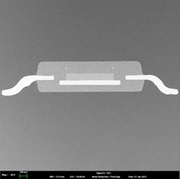 Sectional structure
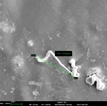 Whisker
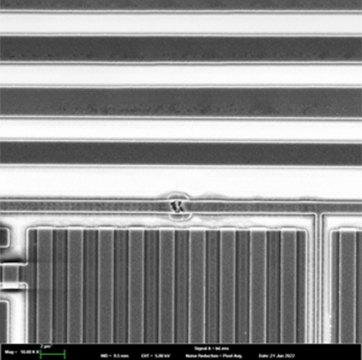 Micro defect detection
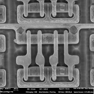 Process
© Raon Solution. ALL RIGHTS RESERVED.